404 Not Found
Nanopolis Suzhou
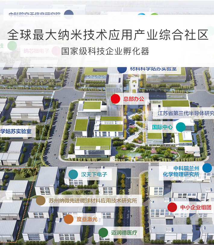
The World's Largest Nanotech Innovation and Industrialization Community
No. 1 MEMS Park in China
Located in China-Singapore Suzhou Industrial Park(SIP), Nanopolis Suzhou is developed and constructed by Nanopolis Suzhou Co., Ltd. It consists of Block I, Block II and Block III and takes up a land area of nearly 1,800 mu (a Chinese unit of area, 1 mu equals to 0.07 hectare). Till December 2020, it has completed the construction of approx. 500,000 m2, gathered 250+ leading talents at various levels, and received a lot of honors, such as National S&T Business Incubator, State-level Featured Carrier of Leading Talents, National Demonstration Unit of Public Service for Overseas Chinese Returnees, State-level Innovation and Entrepreneurship Base of All-China Federation of Returned Overseas Chinese and National Exemplary Industrial Park of Harmonious Labor Relationship, etc.
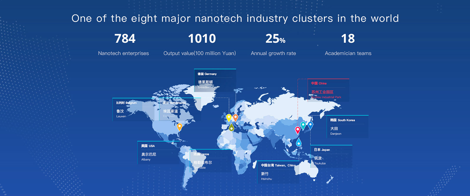
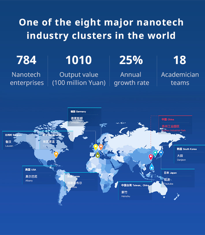
Known as the world's largestcommunityof nanotech innovation and industrialization today, Nanopolis Suzhou ishome to 460+ nanotech firms among a total of 780+ that are settled in SIP.
Learn moreNanopolis Suzhou
The World's Largest Nanotech Innovation and Industrialization Community
No. 1 MEMS Park in China
Located in China-Singapore Suzhou Industrial Park(SIP), Nanopolis Suzhou is developed and constructed by Nanopolis Suzhou Co., Ltd. It consists of Block I, Block II and Block III and takes up a land area of nearly 1,800 mu (a Chinese unit of area, 1 mu equals to 0.07 hectare). Till December 2020, it has completed the construction of approx. 500,000 m2, gathered 250+ leading talents at various levels, and received a lot of honors, such as National S&T Business Incubator, State-level Featured Carrier of Leading Talents, National Demonstration Unit of Public Service for Overseas Chinese Returnees, State-level Innovation and Entrepreneurship Base of All-China Federation of Returned Overseas Chinese and National Exemplary Industrial Park of Harmonious Labor Relationship, etc.
Known as the world's largestcommunityof nanotech innovation and industrialization today, Nanopolis Suzhou ishome to 460+ nanotech firms among a total of 780+ that are settled in SIP.
Learn more-
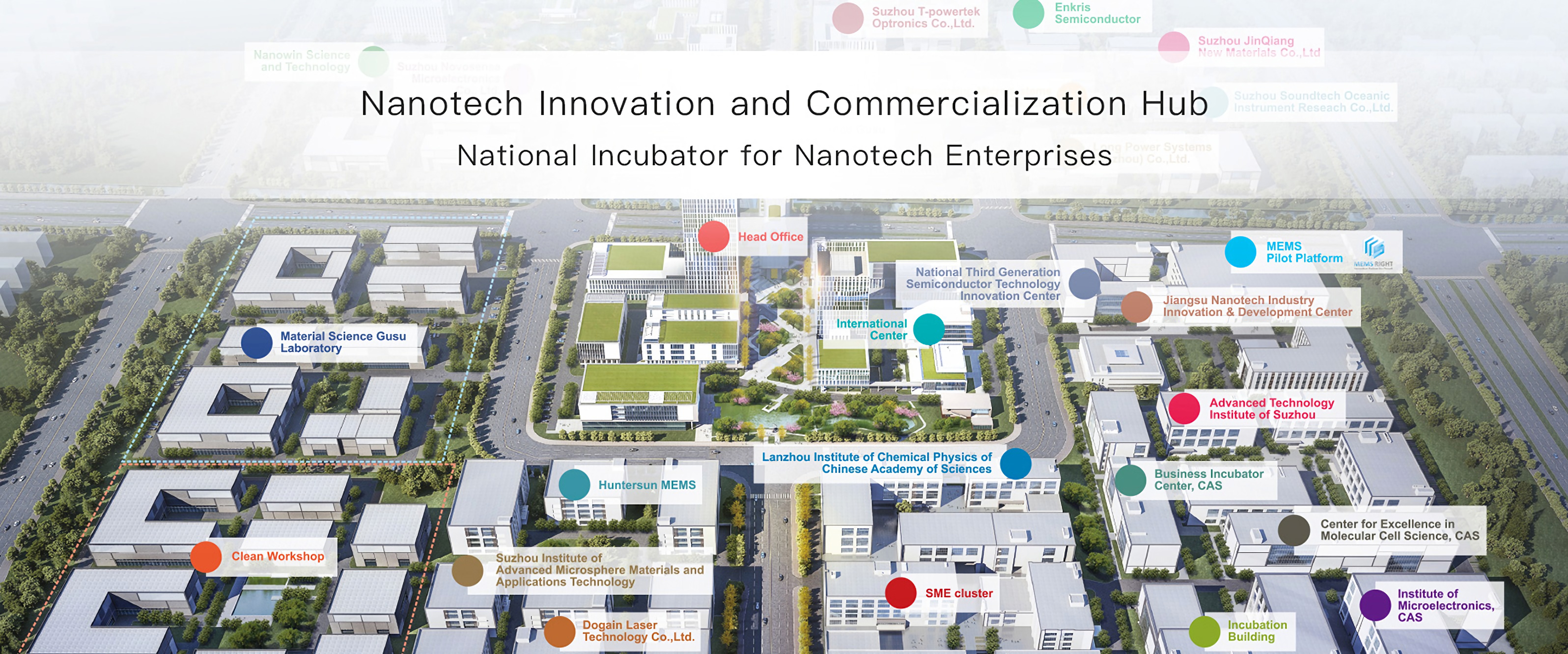
Innovation and R&D
Shown as building clusters of innovation and R&D, Nanopolis Suzhou can meet various needs of nanotech firms, from R&D, pilot production to offices. Generally, the first floor is 6 meters high, the second floor 5 meters high and the third to fifth floors 4.2 meters high; passenger and freight elevators are both equipped.
-
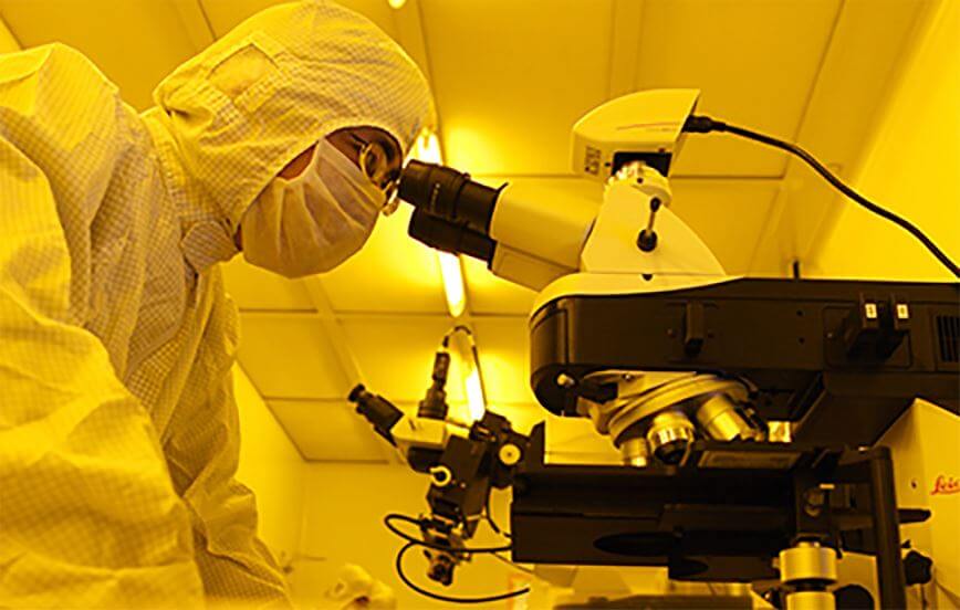
Pilot platform
Nanopolis Suzhou has built the first commercialized operated, 6-inch MEMS pilot platform in China. It has 3,000 square meters of 6-inch high standard clean workshop, more than 170 sets of MEMS specialized processing equipment, and an accumulated investment of more than 500 million Yuan.
-
Factory buildings
A cluster of factoriesbuildings mainly serves medium sized manufacturing enterprises (SEM) in the nanotechnology industry. With adequate consideration given to the SME's needs of space utilization, transfer path and rental cost during its design stage, it features convenient freight passage and flex rooms for optimized space utilization.
-
Project incubation
Mainly used for early and middle-stage incubation of nanotech innovation projects. Those projects with good market prospect and clear industrialization direction and model will be given a variety of incubation services, including financial support, free office space and pilot production platform subsidies, etc.
-
Industry service
Equipped with specialized industry service team, Nanopolis Suzhou facilitates enterprises in matters related to enterprise fitment and settlement, investment and financing, project application, intellectual property, pilot platform support, international collaboration, technology transfer, etc. in accordance with the inherent needs of enterprises at start-up, growth, scale development and other stages.
-
Headquarter office
Nanopolis Suzhou has gathered a broad range of industrial resources and service institutions regarding R&D, pilot test, production and investment, etc. that can provide strong support to the settlement of companies’ headquarters. Two high-standard, over 100 meters high office buildings are being built in the central area to provide ideal headquarter office environment for the development of large-scale enterprises.
-
Conference &Exhibition
With focus on the achievements and products of nanotech innovation in SIP and Nanopolis, it serves as a specialized exhibition platform that integrates product applications exhibition, demonstration and cooperation and exchange.
-
Commercial Facilities and Amenities
With good dining atmosphere and a variety of dishes, different types of dining services are available to meet various needs such as working meal or business reception, etc.; coffee shops, convenience stores, banks, fresh distribution, car wash, etc. are also equipped to make sure your needs are met.
Industry Service
.jpg)

.jpg)

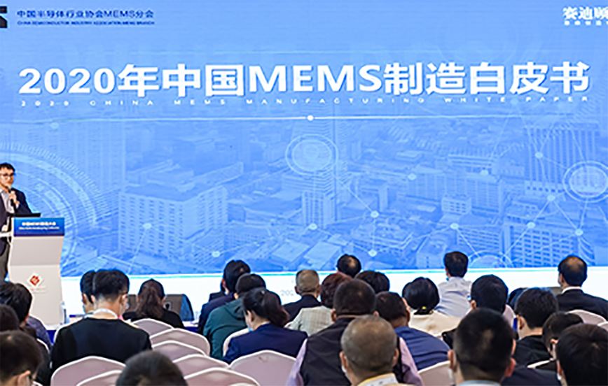
Industry focus
Buiding the MEMS Industry Ecosystem at full power. Focused on realizing an "R&D-pilot-production" integrated MEMS platform to fill the market gap. Home to nearly 100 MEMS enterprises to form the ...
National Innovative Industrial Cluster Pilot for Nano New Materials Focused on the development of advanced materials such as carbon nanomaterials (graphene, fullerene, carbon nanotubes), nano ...
Fostered a batch of leading 3rd generation semiconductor enterprises, including Nanowin, Enkris, Focuslightings, Suzhou Gpower,Suzhou Nengwu (苏州能屋), Suzhou Alighting, etc. in possession of ...
Focused on the development of four key sub-sectors, i.e., health management and monitoring, health care, detection and diagnosis and medical devices Nearly 100 nano health enterprises are ...
About US
.png)

About us

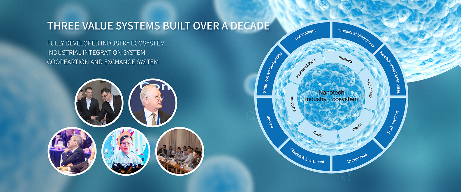
Nanopolis Suzhou Co., Ltd. is a state-owned enterprise directly under Suzhou Industrial Park. Founded in 2010, it is the main driving force of the development of nanotech applications in Suzhou Industrial Park. With three wholly-owned subsidiaries and six joint-stock companies, it focuses on six types of business, i.e., const...
[Celebrities] Comments
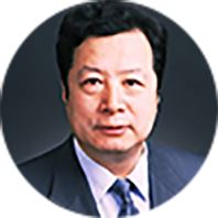
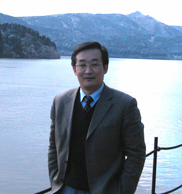
Zhuangde Jiang
Academician of Chinese Academy of Engineering
.jpg)
Suzhou Industrial Park has ascended to one of the top eight nanotechnology communities in the world, become a realHIGHLAND of the nanotechnology industry in China. It is a very rare achievement.

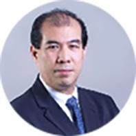
Jinding Yan
Director / Research Fellow, High Tech Center of MOST
It is booming and flourishing of nanotechnology industry in SIP. SIP has become the highland of nanotechnology innovation, as well as industrialization in both China and the world.
Qiang Deng
Secretary of Party Committee / Deputy Director, SINANO CAS
During its development, SIP has precisely seized the directions of the industry development,arranged layout of industrial chain wisely with various supporting policies, and formed an industry cluster with full chain that includes from upstream materials to downstream manufacturing by meticulous care.
Ke Xu
President of Jiangsu Institute of Advanced Semiconductors
Suzhou Industrial Park has formed the industrial agglomeration incentivized by talent pooling, and the integrative development of science and technology, financing and public support platforms. In the field of high-end GaN technology, most of our exclusive, original achievements and world-leading tech teams are settled in Suzhou Industrial Park.
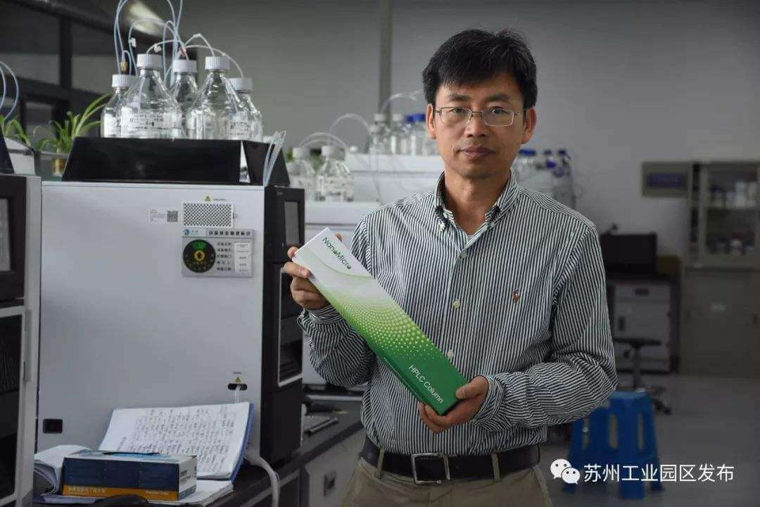
Biwang Jiang
Chairman, Suzhou Nano Micro Technology Co., Ltd. The only company in the world of producing monodisperse silica gel chromatographic packing on a large scale
It is the beneficial startup and innovation environment in SIP,as well as the government's strong support that enables Nano Micro to grow rapidly and become a global leader in the field of microsphere manufacturing.
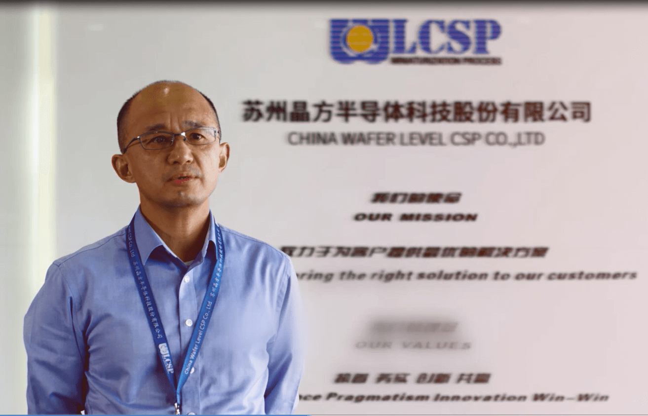
Wei Wang
Chairman / General Manager of China Wafer Level CSP Co., Ltd. The world's leading wafer-level chip scale package on a mass scale
SIP has a healthy political environment and provides you with a beneficial package of support, including industrial chain and the ecosystem, to offer you a desired advantage for company development.
Niancai Peng
Chairman of Xi'an Tianlong Science and Technology Co., Ltd. A leader of innovation in the field of gene detection and molecular diagnosis in China
The reason that Tianlong Science and Technology put the reagent which has the highest output value and the most critical future development of the molecular diagnosis system in Suzhou is our recognition and trust to Suzhou and Suzhou Industrial Park.
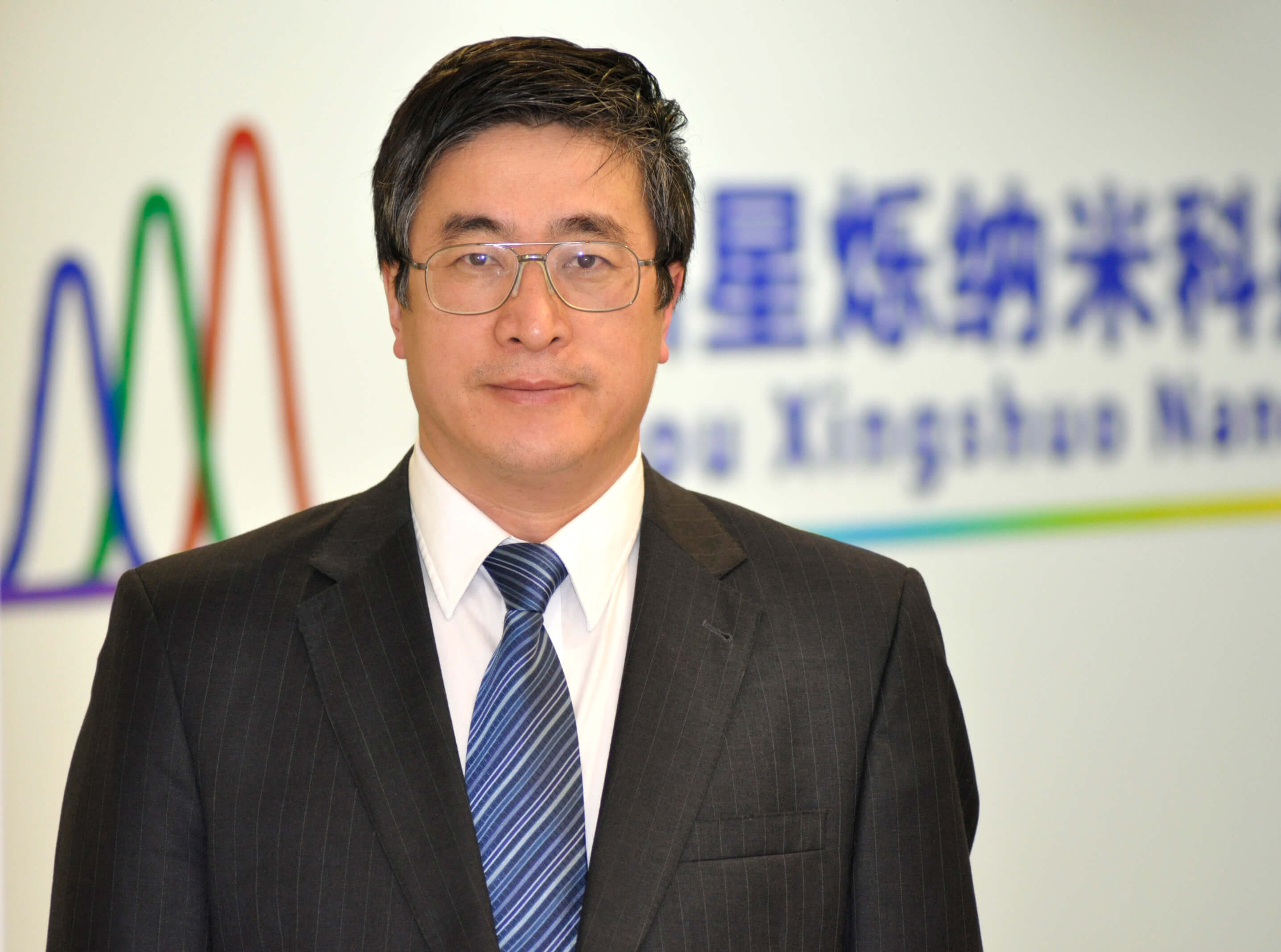
Yunjun Wang
Chairman of Suzhou Xingshuo Nanotech Co., Ltd. Focused on the R&D and industrialization of new fluorescent nanoparticles (quantum dots)
In 2012, I returned to Suzhou from the United States, hoping to use our quantum dot technology to promote the technological upgrading of China's display industry.
Kai Cheng
Chairman of Enkris Semiconductor Inc. China's only, World’s leading manufacturer of large-diameter GaN epitaxial wafer on silicon substrate
It's been nearly ten years since we started business in Suzhou. Today, Enkris Semiconductor has become China's only, world’s leading manufacturer of large-diameter GaN epitaxial wafer onsilicon substrate.
Zhuangde Jiang
Academician of Chinese Academy of Engineering
Suzhou Industrial Park has ascended to one of the top eight nanotechnology communities in the world, become a realHIGHLAND of the nanotechnology industry in China. It is a very rare achievement.

Jinding Yan
Director / Research Fellow, High Tech Center of MOST
It is booming and flourishing of nanotechnology industry in SIP. SIP has become the highland of nanotechnology innovation, as well as industrialization in both China and the world.
Qiang Deng
Secretary of Party Committee / Deputy Director, SINANO CAS
During its development, SIP has precisely seized the directions of the industry development,arranged layout of industrial chain wisely with various supporting policies, and formed an industry cluster with full chain that includes from upstream materials to downstream manufacturing by meticulous care.
Ke Xu
President of Jiangsu Institute of Advanced Semiconductors
Suzhou Industrial Park has formed the industrial agglomeration incentivized by talent pooling, and the integrative development of science and technology, financing and public support platforms. In the field of high-end GaN technology, most of our exclusive, original achievements and world-leading tech teams are settled in Suzhou Industrial Park.
Biwang Jiang
Chairman, Suzhou Nano Micro Technology Co., Ltd. The only company in the world of producing monodisperse silica gel chromatographic packing on a large scale
It is the beneficial startup and innovation environment in SIP,as well as the government's strong support that enables Nano Micro to grow rapidly and become a global leader in the field of microsphere manufacturing.
Wei Wang
Chairman / General Manager of China Wafer Level CSP Co., Ltd. The world's leading wafer-level chip scale package on a mass scale
SIP has a healthy political environment and provides you with a beneficial package of support, including industrial chain and the ecosystem, to offer you a desired advantage for company development.
Niancai Peng
Chairman of Xi'an Tianlong Science and Technology Co., Ltd. A leader of innovation in the field of gene detection and molecular diagnosis in China
The reason that Tianlong Science and Technology put the reagent which has the highest output value and the most critical future development of the molecular diagnosis system in Suzhou is our recognition and trust to Suzhou and Suzhou Industrial Park.
Yunjun Wang
Chairman of Suzhou Xingshuo Nanotech Co., Ltd. Focused on the R&D and industrialization of new fluorescent nanoparticles (quantum dots)
In 2012, I returned to Suzhou from the United States, hoping to use our quantum dot technology to promote the technological upgrading of China's display industry.
Kai Cheng
Chairman of Enkris Semiconductor Inc. China's only, World’s leading manufacturer of large-diameter GaN epitaxial wafer on silicon substrate
It's been nearly ten years since we started business in Suzhou. Today, Enkris Semiconductor has become China's only, world’s leading manufacturer of large-diameter GaN epitaxial wafer onsilicon substrate.
Contact us
Partnership
.png)


404 Not Found

Your request was successfully sent